
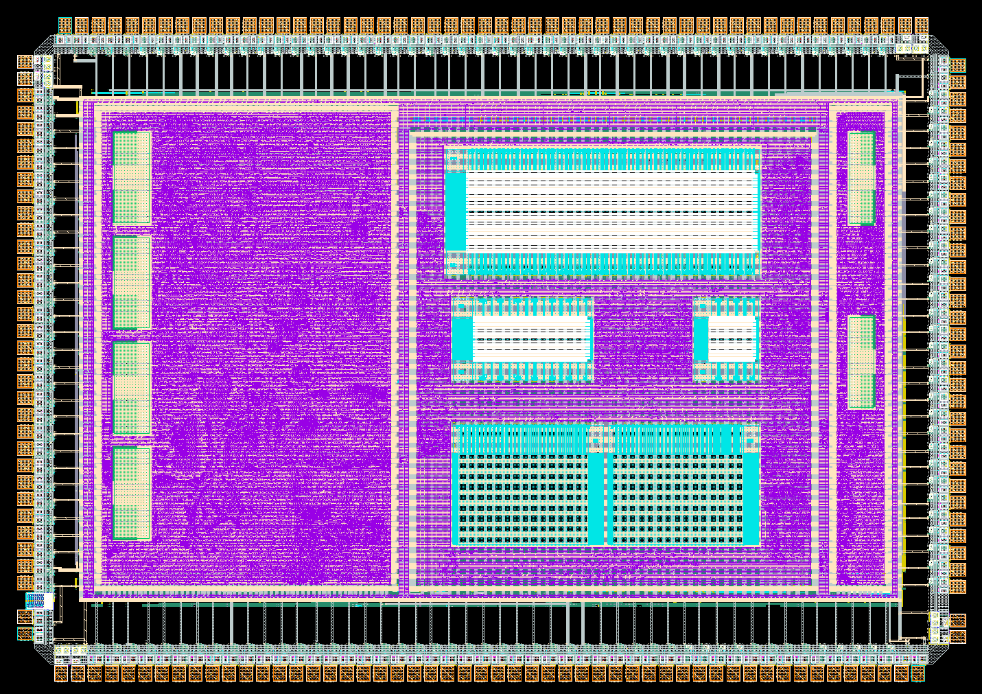
Top level chip layout
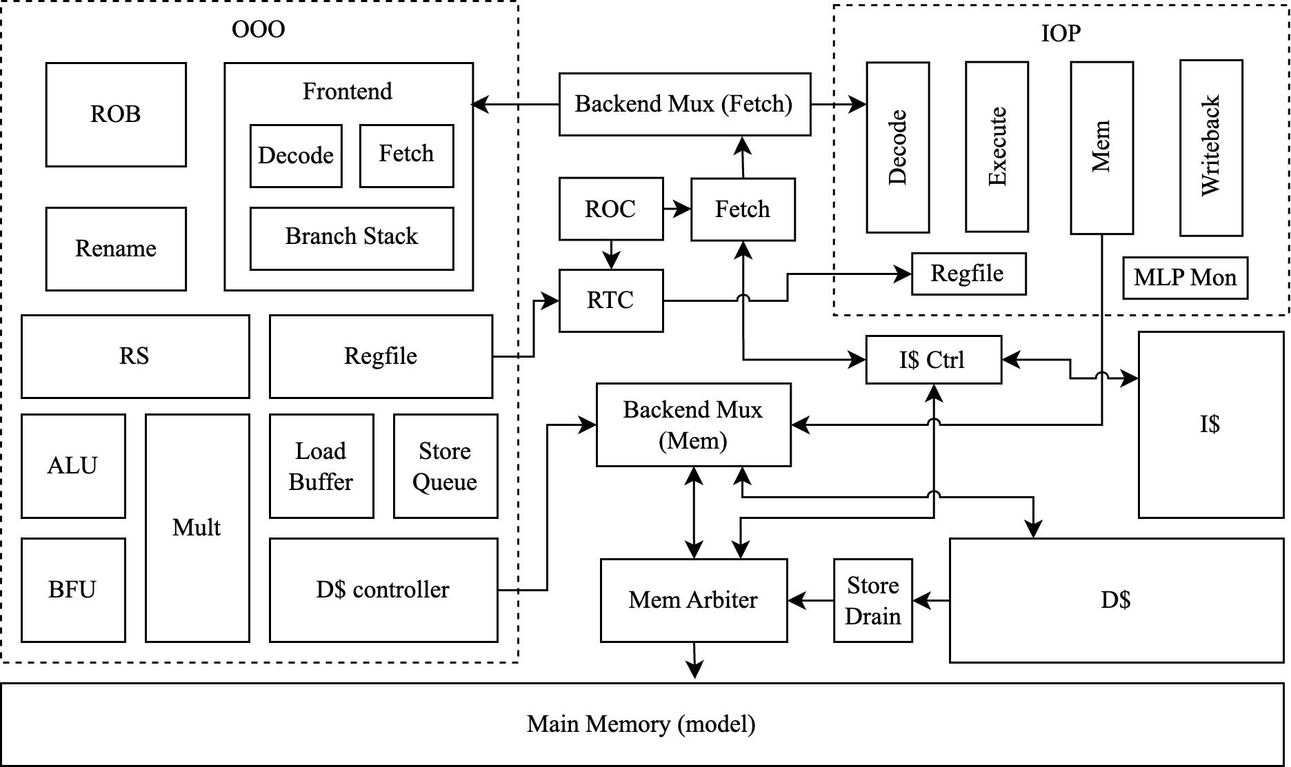
Top level functional diagram
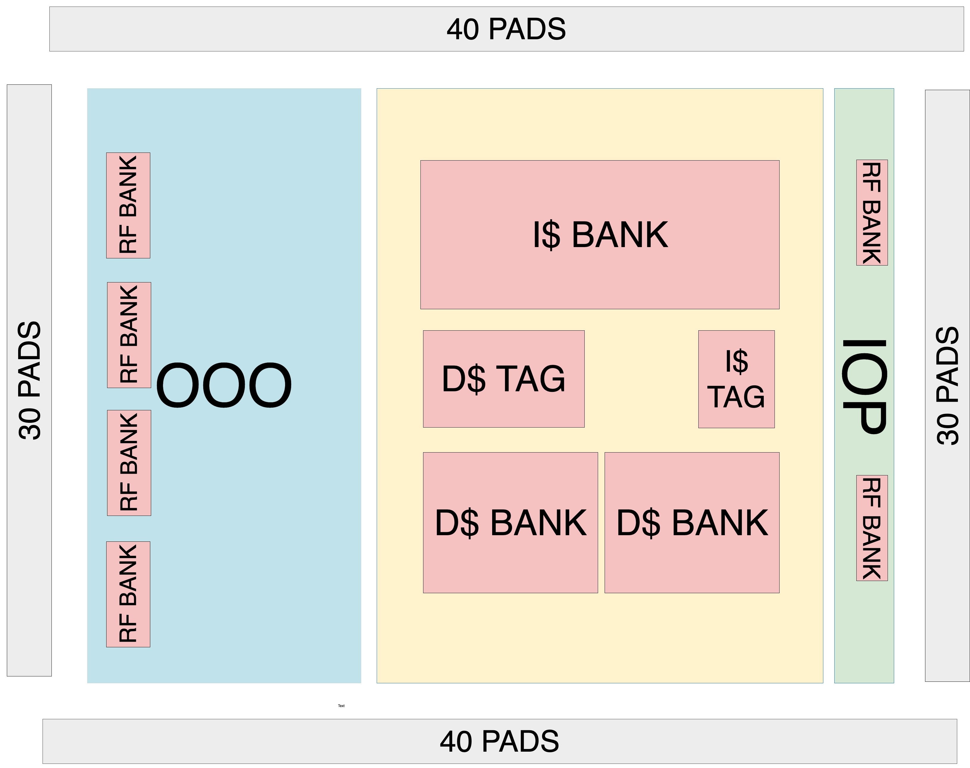
Top level floorplan
Project information
- Category: VLSI
- Completion date: April 2025
- Technologies: Verilog, Cadence, TSMC 180nm
Details
My group project in EECS 627: VLSI Design II at the University of Michigan was a heterogeneous processor implemented in TSMC 180nm technology that supports fine-grained context switching between a performance out-of-order core and a power efficient in-order core. Both backends share a branch predictor, instruction cache, and data cache so that only the register file contents must be transferred on a context switch. Switching between backends takes less than 40 cycles and can occur up to every 1000 instructions.
I designed, implemented, and tested the out-of-order backend. This backend features single-cycle branch recovery, pipelined issue for back-to-back execution of dependent instructions, a multi-ported register file, and custom data cache controller to support multiple simultaneous out-of-order loads and stores. I also implemented the central always-on domain containing instruction fetch (with a gshare branch predictor), and backend multiplexing logic.
Our project report is available here